
MNIS
Micro Nano Integrated Systems Lab
Research
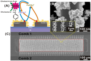
Biosensors based on electrical-double-layer field-effect transistors (EDL FET)
1. Motivation

Biosensors have emerged as powerful tools for the detection of biomolecules, such as proteins, DNA, and cells, in biological fluids. They have broad applications in healthcare, environmental monitoring, food safety, and biodefense. Depending on the sensing scheme, biosensors can be classified into optical, electrochemical, mass-based, and field-effect-transistor (FET) biosensors. Among these, FET biosensors have gained significant attention due to their label-free, real-time, and sensitive detection capabilities. The ion-sensitive field effect transistor (ISFET) was one of the first FETs developed for biosensor applications. ISFETs are known for their fast response and high sensitivity to biomolecules. The major problem in biomolecule sensing with ISFETs is the Debye screening effect, which has been overcome by diluting biofluid samples. However, there is significant interest in developing FET biosensors operating without the need for a dilution process.
The electrical-double-layer field-effect-transistor (EDL FET) biosensor has gained significant interest in recent years as a promising device to solve the Debye screening effect problem. By applying a high electric field to the gate, which is modified with a biomolecule receptor, an electrical double layer (EDL) forms on the surface of the gate and channel. Thus, the formation of the EDL changes the current (Drain-Source) in the channel. In this scheme, the EDL does not interfere with the sensing performance but rather contributes to it. The EDL FET biosensor has several advantages over ISFETs, including higher sensitivity to charged biomolecules, a wider dynamic range of detection, and robustness in varying pH and ionic strength conditions.
2. Approach: Suspend gate-integrated EDL FET biosensor

We are developing suspended gate-integrated EDL FET biosensors. The suspended gate is positioned above the FET channel by a few micrometers. Therefore, this small gap generates a high electric field, even when a low voltage is applied; this allows for highly sensitive measurement of target biomolecules while preventing unnecessary electrochemical reactions and reducing the power required to operate the sensor. The suspended gate electrode is fabricated in the form of a nano-sized mesh, which allows for dense immobilization of bio-receptors due to its large surface area. Moreover, the target biomolecules can be easily supplied to the surface of the gate electrode through the cavity of the mesh, enabling high-sensitivity measurements. Using the cost-effective C-MEMS technology, the suspended mesh structure can be easily fabricated at the wafer level. Additionally, we are maximizing the sensor performance by selectively modifying the surface of the gate electrode without affecting the semiconductor surface. We expect the suspended mesh gate-integrated EDL FET biosensor to be widely utilized in the detection of various biomolecules due to its agility, cost-effectiveness, label-free detection, simple sample preparation, and high sensitivity.
Non-enzymatic glucose (NEG) sensor
1. Motivation

5.37 billion people, which is 6.7% of the global population, are suffering from diabetes in 2021, and this number is projected to increase to 7.83 billion by 2045. Diabetes is a chronic disease, and it requires continuous blood glucose monitoring due to its difficulty in curing and the presence of serious complications. Blood glucose meters on the market have the advantages of high accuracy and low cost, but they require frequent measurements of 4-8 times a day, and users must endure the pain of pricking their fingers each time. Recently, invasive type continuous glucose monitoring devices have been growing in popularity. However, they are less accurate than blood glucose meters, expensive, and still require needles to be inserted into the skin. Both methods require needles to be inserted into the body, which has limitations in terms of user discomfort and can decrease their willingness to monitor their blood glucose. To address these issues, non-invasive glucose sensors are actively being researched. Non-invasive glucose sensors use the fact that the glucose concentration in body fluids is proportional to that in blood to predict blood glucose levels by measuring the glucose concentration in body fluids (e.g., sweat, saliva, tear). However, since the glucose concentration in body fluids is about 1/20 of that in blood, highly sensitive glucose detection is essential. Non-enzymatic glucose sensors have excellent long-term safety because they do not use enzymes. However, they require a highly porous electrode for high selectivity and an alkaline environment for high sensitivity. Therefore, many researchers of non-enzymatic glucose sensors use a porous electrode structure with pre-processing of the sample to increase the pH to create an alkaline media or use complex fluid systems.

2. Approach : Non-enzymatic glucose sensor with high sensitivity and selevtivity
We are developing a glucose sensor with high sensitivity and selectivity by utilizing a nanoporous carbon structure fabricated by C-MEMS. Using the dewetting process, gold nanoparticles, which work as catalysts toward glucose, form densely on the porous carbon electrode. In addition, a pH modulation electrode is integrated next to the glucose sensing electrode (nanoporous carbon electrode) to locally increase the pH without pre-treatment, allowing for highly sensitive glucose measurement. Furthermore, pH modulation is confined to the proximity of the working electrode, allowing glucose measurement without skin irritation even when the sensor chip is attached close to the skin. All electrodes are fabricated using MEMS processes, enabling the low-cost production of micro-scale electrode systems at a wafer level. In addition, we are developing an electrochemical filtering system, ensuring high selectivity.
Enzymatic electrochemical biosensors and immunosensors
1. Motivation
Development of sophisticated bioassay platforms which allow instantaneous and precise concentration measurement of analyte is essential for advancement of biosensors. Among various types of biosensors, enzymatic electrochemical biosensors are acclaimed for their wide dynamic range, high selectivity, and accurate sensing. Such biosensor combines sensing technology with a specific response to enzyme-product reaction. Thus, labeling of a sensing element with a particular protein enhances sensitivity and selectivity of a sensor. To further amplify signal from target analyte and biorecognition element interaction, redox cycling method is used. When oxidizing and reducing electrodes are in tight proximity, their diffusion layers overlap, and redox mediators undergo oxidizing and reducing reactions repeatedly before diffusing out to the bulk solution. Hence, signal amplifies. In order to localize enzyme close to the active electrode surface and to make narrow spacing between electrodes, precise control fabrication techniques have been developed. Simple and cost-effective C-MEMS technology allows various manipulations of electrodes’ design. Configuring electrode geometry in sub-micrometer level boosts its surface to volume ratio and reduces required sample volume. Consequently, enhanced signal amplification enables versatile integration of 3D micro/nano structures for electrochemical biosensing.
2. Approach: Selectively functionalized 3D electrodes for hypersensitive electrochemical biosensing
We developed selective enzyme immobilization technique on high aspect ratio on-plane structures and suspended structures. By controlling the spacing between the functionalized electrode surface and active electrode surface, the product from enzyme-analyte reaction swiftly diffuses and gets oxidized with redox mediator adjacent to a sensing electrode surface. The concept explained above was used for selectively attaching proteins on electrode arrays with large surface volumes for sensing cholesterol, glucose, or uric acid levels from the solution. The method has also shown its application in immunosensing with low LOD, high sensitivity, and selectivity.
Currently, we are working on precise fabrication control of the electrodes in nanoscale to advance electrodes’ performance to the next level.

Reference
-
Sharma, Y. Lim, Y. Lee, H. Shin**, Glucose sensor based on redox-cycling between selectively modified and unmodified combs of carbon interdigitated array nanoelectrodes, Analytica Chimica Acta 889 (2015) 194-202.
-
Sharma, J. Lee, H. Shin**, An electrochemical immunosensor based on a 3D carbon system consisting of a suspended mesh and substrate-bound interdigitated array nanoelectrodes for sensitive cardiac biomarker detection, Biosensors and Bioelectronics 107 (2018) 10-16.
-
Sharma, J. Lee, J. Seo, H. Shin**, Development of a sensitive electrochemical enzymatic reaction-based cholesterol biosensor using nano-sized carbon interdigitated electrodes decorated with gold nanoparticles, Sensors 17 (2017) 2128.
TSV packaging for C-MEMS devices

1. Motivation
C-MEMS is a non-conventional batch fabrication technology enabling cost-effective manufacturing of 3D micro/nano carbon structures at a wafer level by pyrolyzing pre-patterned polymer structures. Due to 3D hybrid-scale structure, excellent mechanical robustness, electrical conductivity, and chemical inertness, C-MEMS-based carbon structures have been actively studied to develop various miniaturized systems such as gas sensors, biosensors, environmental sensors, Li-ion batteries, and microfluidic devices. Recently, the through-silicon via (TSV), one of the advanced packaging technologies, has been attracting attention to improve the performance of MEMS device chips. TSV is a packaging method of manufacturing an electrical passage through the Si wafer, enhancing power saving, miniaturization, and fast signal transmission compared to the previous wire-bonding-based packaging. Nevertheless, since C-MEMS-based devices are accompanied by a high-temperature pyrolysis process (600~1200 °C), the conventinal TSV technologies are limited to be applied to the C-MEMS process.
2. Approach
We are developing a novel TSV packaging technology adaptive to C-MEMS devices. The TSV packaging method consists of three main steps; forming a hole penetrating the substrate, integrating the target C-MEMS device, and coating/filling the via inside with a conductive material. Therefore, the conductive material coated in the via is not exposed to a high-temperature pyrolysis process, preventing via fracture problems caused by the CTE mismatch and low melting temperature of the conductive coating material (e.g., metal, conductive polymer). Since the MEMS process involves multiple wet steps, such as photolithography and lift-off, a strategy is required to protect empty vias from contamination or blockage. To facilitate the integration of C-MEMS devices without via contamination, we seal the top inlet of the void vias with a thin pyrolyzed carbon film before the C-MEMS-device integration. Owing to the good mechanical properties and chemical inertness, the carbon film protects vias without deformation, even in various wet processes and high-temperature conditions. In addition, the pyrolyzed thin carbon film ensures a good electrical connection between the MEMS devices and the via fillers.
Nanoheater enabled ultralow-power sensor devices

1. Motivation
Various 1D nanomaterial (e.g., nanowire, nanotube)-based heater structures have been proposed to improve the power efficiency of electrothermal devices due to their high aspect ratio and small size. However, their use has been limited by the drawbacks of nanoscale manufacturing technologies such as high cost and complex process.
2. Approach
A novel wafer-level batch fabrication method of suspended 1D nanoheaters (diameter: sub-micrometer, length: 50–150 mm) has been developed. The suspended 1D nanoheaters ensure superior heat confinement, enabling ultralow-power operation. The developed fabrication method involves suspended carbon nanowire backbone fabrication and subsequent selective metal coating. The fabrication method allows for precise control of the size and shape of the 1D nanoheater; this allows for optimizing its performance and extending its applicability to various electronic devices, such as the Internet of Things (IoT).
2.1. Thermal conductivity detector (TCD)-type gas sensor
Thermal conductivity detector (TCD)-type gas sensors are widely used to detect high-concentration gases or identify low-concentration gases in chromatography, owing to their fast response and recovery time for a wide range of gases. However, conventional TCD devices require large power consumption because of their relatively large sizes, which limits their applicability, specifically in IoT. To overcome this limitation, microscale bridge-type heater-based gas sensors have been developed using MEMS technologies, leading to the reduction in power down to ~ 0.1 mW. However, further power and size reduction require complex nanofabrication technologies limiting mass production.
We developed an ultralow-power TCD for use as a gas sensor by manufacturing a suspended nanoheater via cost-effective wafer-level microfabrication technology (i.e., C-MEMS). The small size, high aspect ratio (~ 270, corresponding to a nanoheater length of 80 µm), and suspended architecture allowed the nanoheater-based gas sensor to operate with high sensitivity and ultrafast response/recovery (time constant of less than 1 μs). The nanoheater-based gas sensor exhibited a linear gas response for various high-concentration gases (H2: 1–20 %, Ar: 1–100 %, He: 1–5 %). This fast response enabled the sensor to operate with pulse-width modulation, reducing the power by 1/1000 (240 nW). Thus, nanoheater-based gas sensors are expected to be used in various portable IoT devices.
Recent research topics are extended to temperature sensors, pressure sensors, and flow sensors based on flexible materials or various suspended structures.
Reference
- W. Cho, T. Kim, H. Shin, H**. Thermal conductivity detector (TCD)-type gas sensor based on a batch-fabricated 1D nanoheater for ultra-low power consumption. Sensors and Actuators B: Chemical, 371, 132541.
- W. Cho, S. Lee, T. Kim, B. Kim, H. Shin**, Low Power High Concentration Gas Sensor Based on 3ω-Method Using a Suspended Nanowire Heater. In Electrochemical Society Meeting Abstracts 237 (No. 31, pp. 2312-2312), 2020.
2.2. Chemiresistor-type gas sensor
The new manufacturing method for suspended 1D nanoheaters has the potential to revolutionize the development of chemiresistor-type gas sensors. Chemiresistor gas sensors detect gases by measuring the change in resistance of a sensing material when it interacts with gas molecules. The sensitivity and selectivity of these sensors depend on the type and size of the sensing material used. 1D nanostructures, such as nanowires, have shown excellent gas-sensing properties due to their high surface-to-volume ratio, which enhances gas adsorption and promotes surface reactions.
However, the implementation of 1D nanostructures as sensing materials in chemiresistor gas sensors has been challenging due to the difficulties associated with their fabrication and integration into the sensing device. The new manufacturing method for suspended 1D nanoheaters provides a promising solution to this problem. The suspended 1D nanoheater can provide the heating required to increase gas adsorption and promote surface reactions.
When the nanowire heater is joule-heated, non-uniform heating can occur, affecting the sensitivity and selectivity of the gas sensor. We recently developed a selective patterning technology; this selective material coating ensures more uniform heating, leading to better gas sensing performance. The low power consumption of the suspended 1D nanoheater also enables the development of portable and wearable gas sensors for IoT applications.
Overall, the implementation of suspended 1D nanoheaters in chemiresistor-type gas sensors has the potential to develop highly efficient and cost-effective gas sensors with a wide range of applications.
Reference
- T. Kim†, S. Lee†, W. Cho, Y. M. Kwon, J. M. Baik, H. Shin, H**, Development of a novel gas-sensing platform based on a network of metal oxide nanowire junctions formed on a suspended carbon nanomesh backbone, Sensors 21 (2021), 4525.
- T. Kim, W. Cho, B. Kim, J. Yeom, Y. M. Kwon, J. M. Baik, J. J. Kim, H. Shin**, Batch Nanofabrication of Suspended Single 1D Nanoheaters for Ultralow-Power Metal Oxide Semiconductor-Based Gas Sensors, Small 18 (2022) 2204078.
- T. Kim, S. Lee, B. Kim, W. Cho, J. Lee, H. Shin**, Suspended Heater Embedded Metal Oxide Nanowire Based Gas Sensor Platform. In Electrochemical Society Meeting Abstracts 237 (No. 28, pp. 2123-2123).
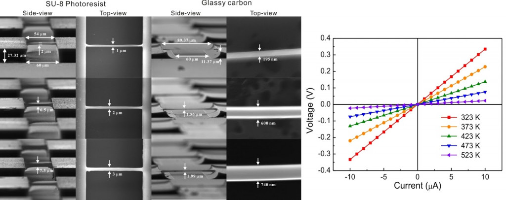
Carbon MEMS
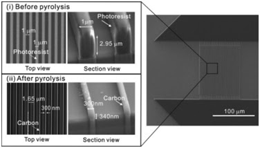
Fabrication of carbon structure through pyrolysis of photoresist structure
: Dramatic size reduction up to ~90 %, highly inert carbon electrode with fancy structure.
1. Electrochemical sensor platform - 1:1 aspect ratio IDA nanoelectrodes
Batch fabrication of interdigitated nanoelectrode array.
- Gap between electrode reduced down to 1.65 μm
- 1:1 aspect ratio (height: 340 nm, width: 300 nm)
- Redox cycling: High electrochemical signal amplification
J. -I. Heo, D. S. Shim, G. Turon Teixidor, S. Oh, M. J. Madou, H. Shin, , “Carbon Interdigitated Array Nanoelectrodes for Electrochemical Applications,” Journal of Electrochemcial Society 158, J76 (2011).
Microchannel
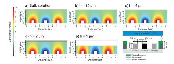
Effect of microchannel height on redox cycling effect of integrated interdigitated carbon nanoelectrode array.
- PDMS channel integration
- Current amplification up to 1116 times.
J. -I. Heo, Y. Lim, H. Shin, “Effect of channel height and electrode aspect ratio on redox cycling at carbon interdigitated array nanoelectrodes confined in a microchannel,” Analyst 138, 6404 (2013).
http://pubs.rsc.org/is/content/articlehtml/2013/an/c3an00905j
Stacked electrode set
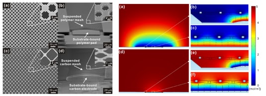
Stacked carbon electrode set including a suspended mesh made of nanowires and a substrate-bound planar electrode.
- Electrode gap reduced down to 2.1 μm
- Unit mesh size: 300–320-nm-wide and 560–600-nm-thick
- Redox current amplification(Ferrocyanide): 37 times
- Dopamine detection down to 5 μM
Y. Lim, J. I. Heo, H. Shin, “Fabrication and application of a stacked carbon electrode set including a suspended mesh made of nanowires and a substrate-bound planar electrode toward for an electrochemical/biosensor platform,” Sensors and Actuators B 192, 796 (2014)
http://www.sciencedirect.com/science/article/pii/S0925400513014159
2. Biosensors - Glucose sensor
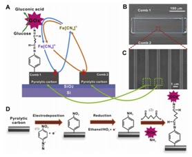
Selective immobilization of enzyme for glucose sensor application. One of the IDA was selectively modified with GOx via the electrochemical reduction of an aryl diazonium salt, while the other comb remained unmodified. Increased active electrode surface resulted in better performance.
- Electrode gap between two combs: 1.9 μm
- Sensitivity enhancement: ~2.3 times
- LOD enhancement: ~295 times
D. Sharma, Y. Lim, Y. Lee, H. Shin* , Glucose sensor based on redox-cycling between selectively modified and unmodified combs of carbon interdigitated array nanoelectrodes, Analytica Chimica Acta, in print.
Biosensor platform: AuNP/C IDA nanoelectrodes
Fabrication of an electrochemical-enzymatic redox cycling-based cholesterol biosensor using 1:1 carbon interdigitated array (IDA) nanoelectrodes decorated selectively with electrochemically deposited gold nanoparticles (AuNPs).
- Nanoparticle size: 50~70 nm
- Sensitivity enhancement: 20~30 %
- LOD enhancement: 2~3 times
3. Gas sensors - Suspended single carbon nanowire as sensor platform
- Full utilization of high surface to volume ratio
- Improved mass transport
- No interference from the substrate
Y. Lim, J. I. Heo, M. J. Madou, H. Shin, “Monolithic carbon structures including suspended single nanowires and nanomeshes,” Nanoscale Research Letters 8, 492 (2013).
http://link.springer.com/article/10.1186/1556-276X-8-492
Suspended single carbon nanowire functinalized with Pd thin film
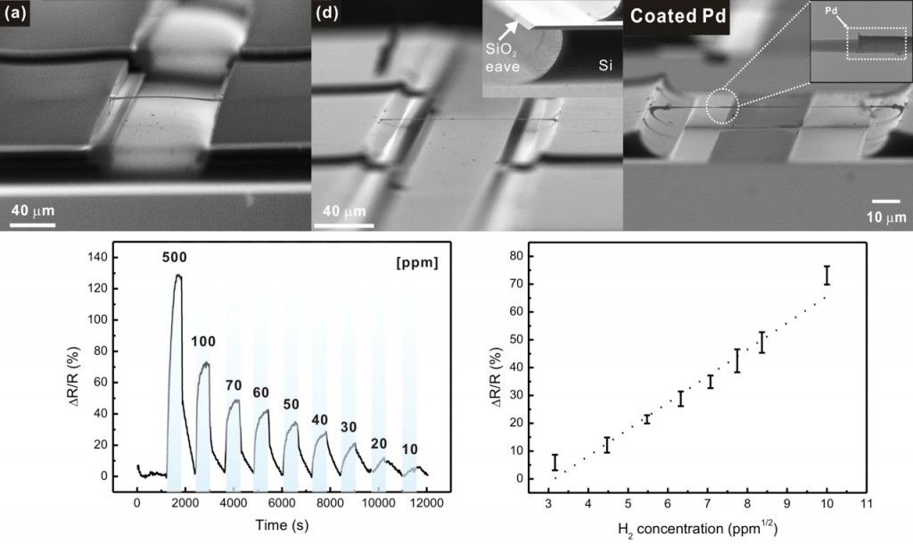
- High hydrogen selectivity
- High sensitivity related to Pd material property
- Room temperature operation
Y. Lim, Y. Lee, J. I. Heo, H. Shin, “Highly sensitive hydrogen gas sensor based on a suspended palladium/carbon nanowire fabricated via batch microfabrication,” Sensors and Actuators B, 210, 218, (2015).
http://www.sciencedirect.com/science/article/pii/S0925400514016554
An array of suspended carbon nanowires functionalized Pd nanoparticles
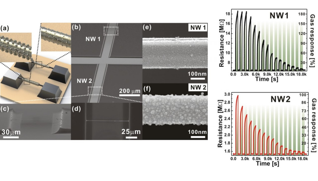
- Controllable Pd nanoparticle morphology
- Wide sensing range according to array structure of nanowires
- High sensing performance according to self-heating effect
- Room temperature operation
Multiplex gas sensor: Suspended MOx NWs
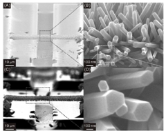
ZnO nanowires were grown selectively on a suspended single glassy carbon nanowire using hydrothermal method so that the detrimental effects from the substrate inclusive of contamination, stagnant layer and limited mass transfer could be alleviated.
- ZnO nanowire diameter: 30~80 nm
- ZnO nanowire length: 0.5~2 μm
Nanoporous carbon
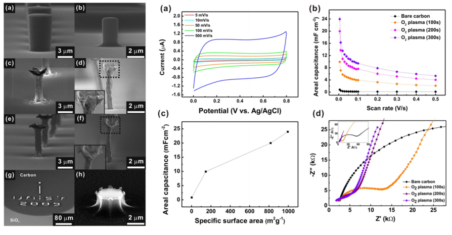
Carbonization of plasma etched polymer precursor
Patternable and controllable multiscale porous 3D carbon structures
- Large surface area & Electric conductivity : Supercapacitors, Sensors, etc.
- Polymer based batch process : Cost-effective
4. Material process RTA - induced conductivity enhancement
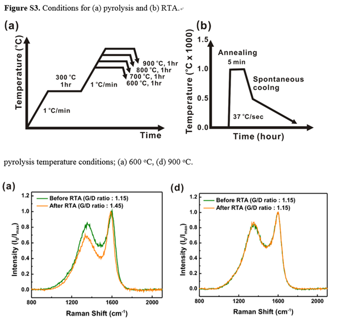
Enhancing the electrical conductivity of GC, so that it can compensate or be substituted for other carbon allotropes such as graphite, carbon nanotubes, and graphene. After the RTA process, the carbon/oxygen content and G-/D-band intensity ratios, which are correlated to the electrical conductivity, were enhanced, depending on the pyrolysis temperature.
- More ordered carbon phase via RTA
- Electrical conductivity enhancement: 3.3 times
5. Micro- and Nano mixed-scale channel networks
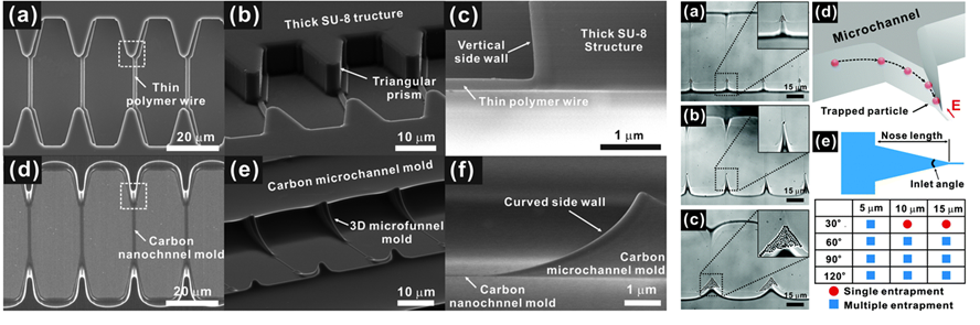
- Channel replication using a monolithic mixed-scale carbon mold PDMS channel networks
- Simple fabrication of mixed-scale polyldimethylsiloxane (PDMS) channel networks via single molding process
- High throughput channel molding process
- Efficient single particle entrapment in Kingfisher-beak-shaped 3D microfunnel
Y. Lee, Y. Lim, H. Shin*, Mixed-scale channel networks including Kingfisher-beak-shaped 3D microfunnels for efficient single particle entrapment, Nanoscale 8 (2016) 11810-11817 (Front cover).
http://pubs.rsc.org/is/content/articlehtml/2016/nr/c6nr00114a
PMMA channel networks
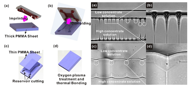
- Simple fabrication of mixed-scale polymethyl methacrylate(PMMA) channel networks via thermal nanoimprint method
- Repeated nanoimprint process owing to mechanically and chemically superb carbon mold.
- Smooth single particle entrapment via diffusiophoresis
SECM-AFM
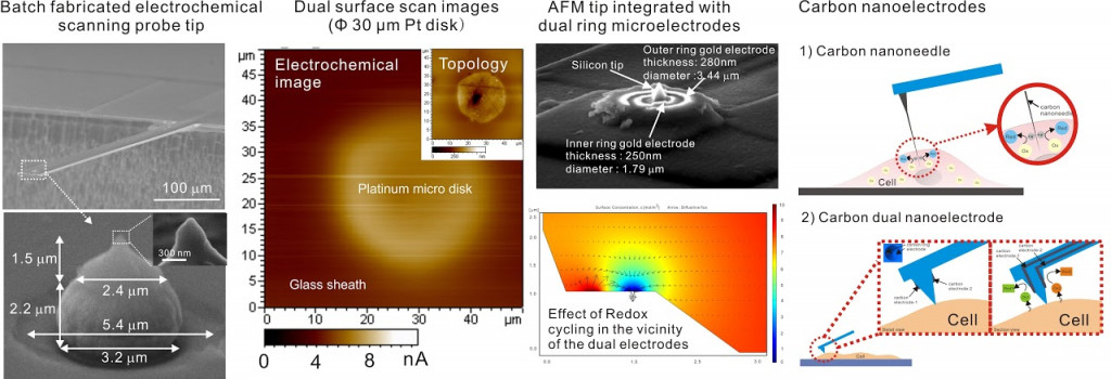
Combination of atomic force microscopy(AFM) and scanning electrochemical microscopy(SECM)
: Simultaneous scanning of topography and electrochemical data of sample surface
Multifunctional Probe
Combined atomic force–scanning electrochemical microscopy
Scanning probe microscopes integrated with dual or single micro/nano electrode
- Simultaneous multiple surface data collection: topology, electrochemical data, pH, biological data, temperature, etc.
- Collection of biological data inside live cells
Conductive Material Nano-Printing
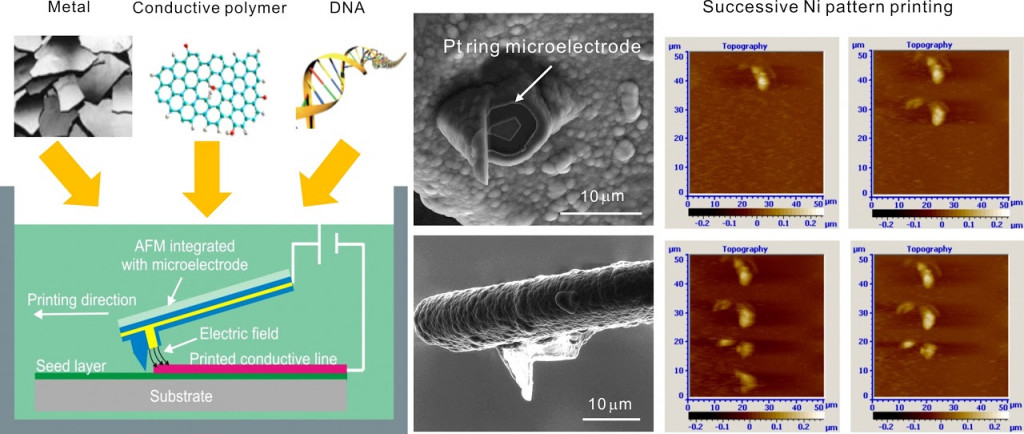
Localized electrochemical deposition of conductive materials using AFM probes
- AFM cantilever tip integrated with micro/nano electrode
- Continuous conductive material printing with high resolution